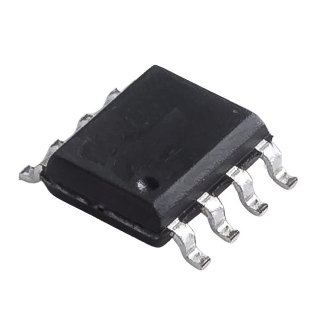
Trench Series, FET, MOSFET Arrays
Results:
3
Manufacturer
Series
Rds On (Max) @ Id, Vgs
Current - Continuous Drain (Id) @ 25°C
Operating Temperature
FET Feature
Configuration
Input Capacitance (Ciss) (Max) @ Vds
Gate Charge (Qg) (Max) @ Vgs
Mounting Type
Supplier Device Package
Vgs(th) (Max) @ Id
Drain to Source Voltage (Vdss)
Package / Case
Technology
Power - Max
Grade
Qualification
Results remaining:3
Applied Filters:
Trench
About FET, MOSFET Arrays
Field-effect transistors (FETs) are electronic devices that utilize an electric field to regulate the flow of current. By applying a voltage to the gate terminal, the conductivity between the drain and source terminals can be modified. Unlike bipolar junction transistors, FETs are unipolar transistors, which means they rely on a single type of charge carrier for their operation. This can either be electrons or holes, but not both. One of the key advantages of FETs is their high input impedance at low frequencies. This property arises due to the fact that the gate terminal of an FET doesn't draw any current, as it's designed to function in a voltage-driven mode. As a result, the input impedance of an FET can be several orders of magnitude greater than that of a similarly configured bipolar transistor. Field-effect transistors come in various types, with the most common ones being Junction FETs (JFETs) and Metal Oxide Semiconductor FETs (MOSFETs). JFETs employ a reverse-biased pn-junction to control the flow of current, while MOSFETs use an oxide layer to insulate the gate from the channel region. FETs have numerous applications in electronics, including amplifiers, switches, oscillators, and voltage regulators. Due to their high input impedance, FETs are often used in circuits where low power consumption and minimal loading effects are crucial considerations. In summary, field-effect transistors (FETs) are electronic devices that utilize an electric field to control current flow. They are unipolar transistors that rely on a single type of charge carrier for their operation. FETs offer high input impedance at low frequencies, making them ideal for use in low power applications where signal quality is a critical factor.


